
In 2018, NXP introduced new MRF101 and MRF300 power transistors to the market. They are designed for medium and high power levels in the radio frequency range, where the offer is not so rich. Why are they extremely interesting to the amateur radio community?
– First of all – they are cheap thanks to the use of standard plastic packages.
– Secondly – they are excellent as a result of the latest LDMOS technology.
– Third – they are easy to design and build both HF and VHF power amplifiers.
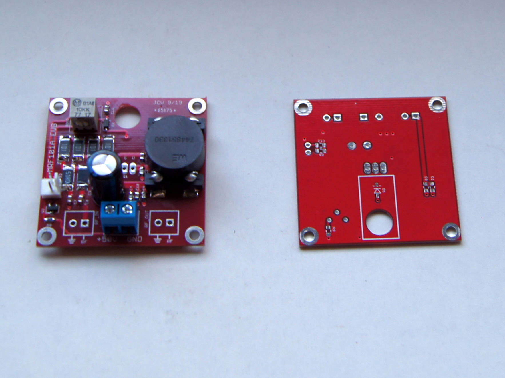
Due to the introduction of these products, NXP announced in May 2019 a competition called “Homebrew RF Design Challenge”. In November 2019, the results were announced – the first place went to Jim WA2EUJ for the solution “An MRF101AN broadband amplifier design with 1 W input, 100 W output, 1.8-54 MHz amplifier deck”. Certainly excellent video helped in winning the competition. Basic project documentation, including a schematic and bill of materials is available HERE. The design is impressive due to its small size, cheapness and ease of implementation. It uses a standard heat sink with a fan to cool processors in desktop computers.
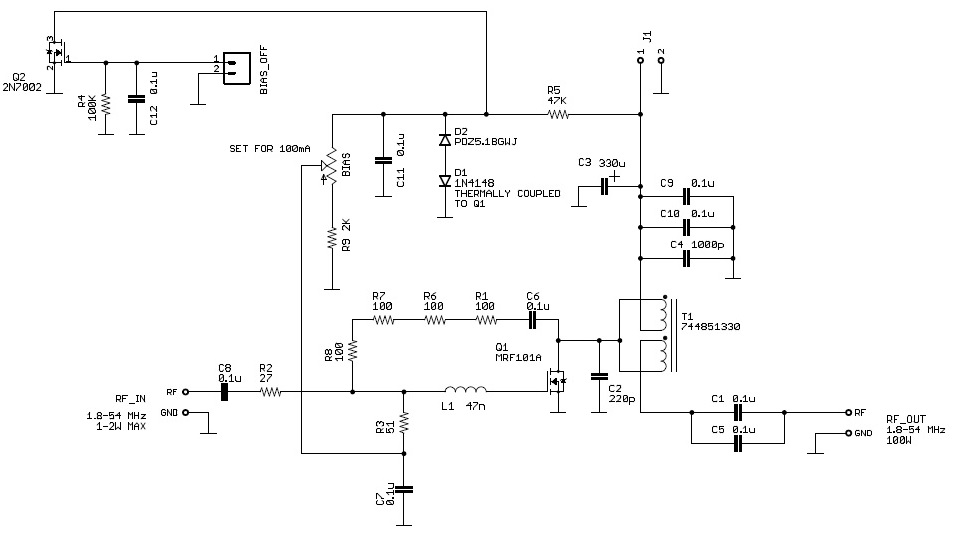
The MRF101_EVB_REV_B version shown above allows the use of PTT, so only it will be discussed further. The simplicity of the schematic is striking. The polarization of Q1 MOSFET gate has thermal compensation by means of the D1 diode. Applying a voltage greater than 3 V to the BIAS_OFF input will turn off the Q1 power transistor. Resistors connected in series with C6 capacitance provide strong negative feedback, very favorable due to the stability and linearity. The output 4: 1 matching transformer is a typical (cheap) common mode choke, often used in power filtering systems. The amazing thing about this choke is how much it simplifies the design of the amplifier. Instead of manually wound coils on ferrite cores, it is enough to solder a ready and easily accessible element on the board …
The MRF101 transistor requires pretty high supply voltage, preferably 50 V. Anyone would like to be able to directly use a typical 13.8 V power supply or battery. But a solution with a high voltage transistor has a lot of advantages. The output impedance of such a transistor is greater, and it is easier to match it to the 50 ohm output. Currents drawn from the power supply are much smaller, so the design can be “softer” and less lossy, without thick traces and wires.
The transistor works in AB class, so non-linear distortions will certainly be greater than in a two-transistor amplifier. As you know, in a perfectly symmetrical push-pull amplifier the even harmonics cancel each other out. This effect does not occur here, i.e. our amplifier can in no case be connected to the antenna without (and a good) bandpass filter at the output.
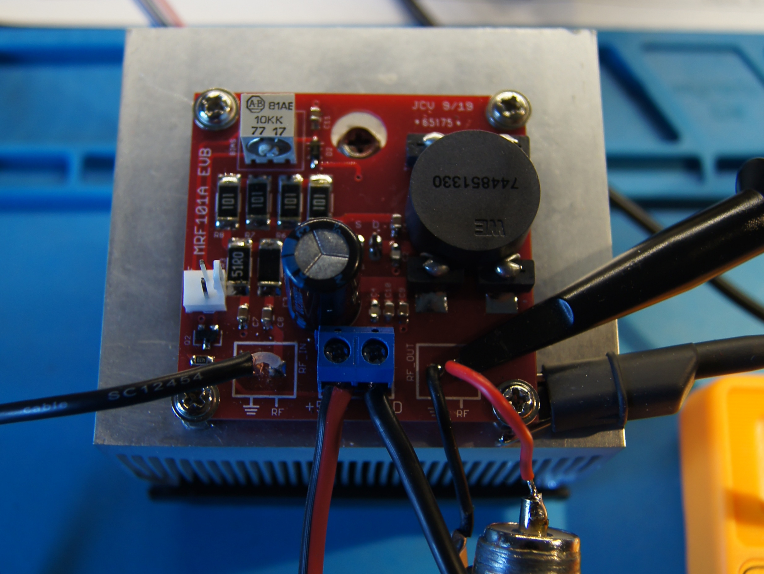
I decided to personally check what this solution is worth and ordered boards and components. The result can be seen below.
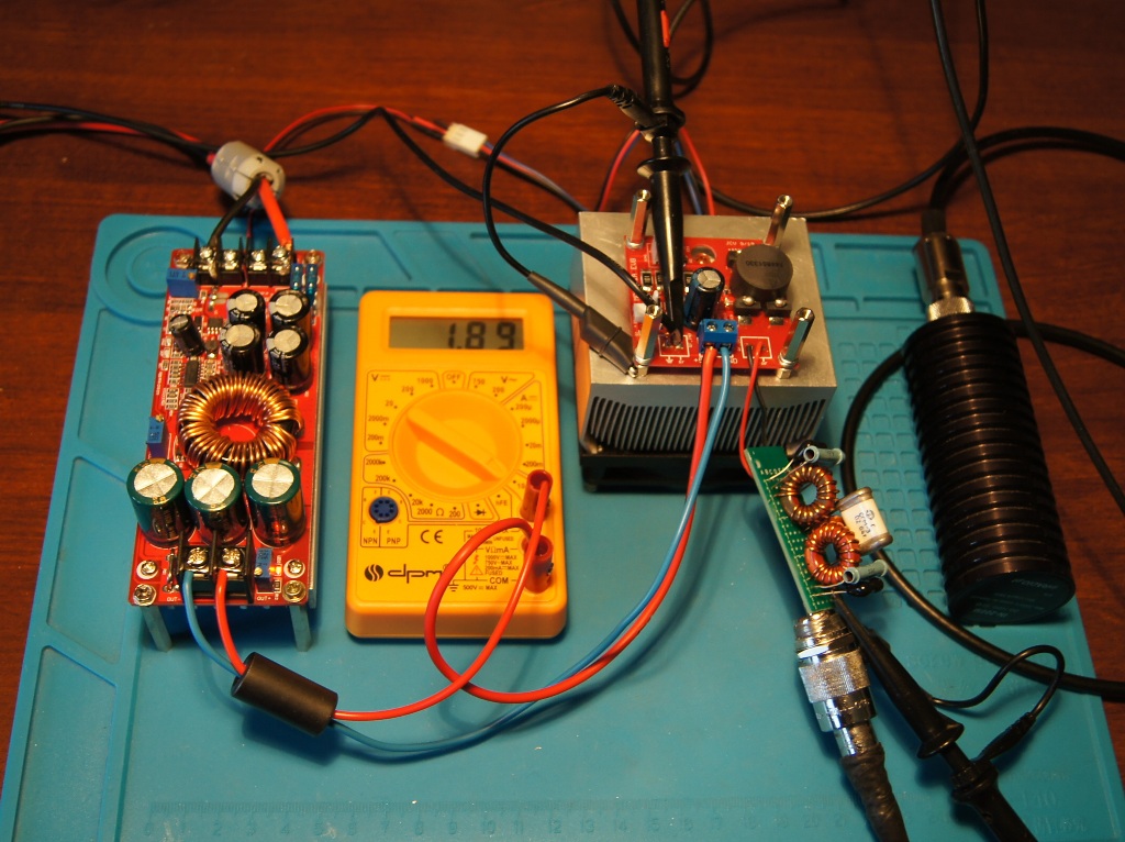
I have assembled the measuring station as in the photo below. The signal source was SunSDR with a 10 dB attenuator. The yellow meter was used to measure the current drawn from the 50 V power supply. An artificial 50 ohm 100 W load and a power indicator (not calibrated) were attached to the output. I used the SDS 1202X-E oscilloscope for measurements. This is a digital oscilloscope with a 200 MHz band and sampling rate of 1 Gs/s. To determine the power on the load, I used the RMS voltage on the load according to the relationship P = U2/R. The manufacturer does not specified the accuracy of the oscilloscope measurement, but assuming that we were dealing with a sampled signal in the digital domain, it should not be worse than 10%.
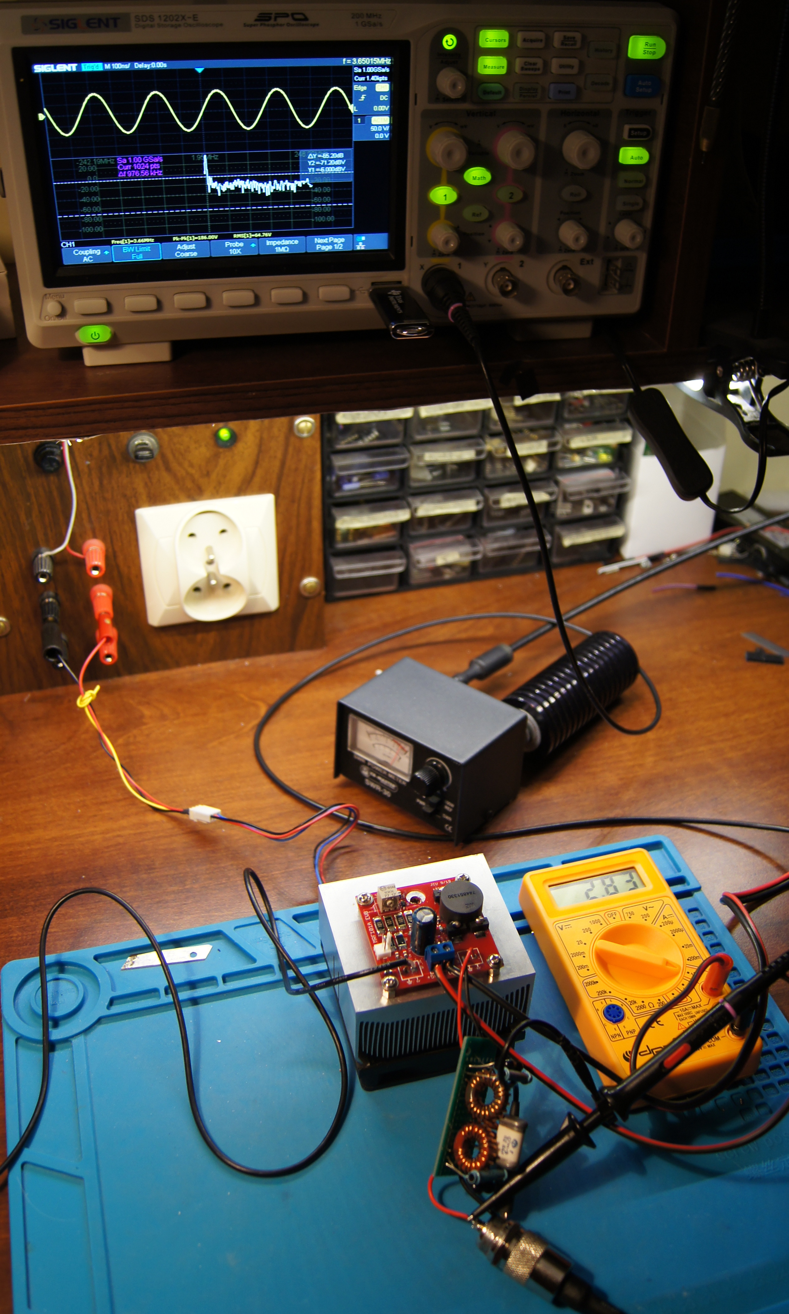
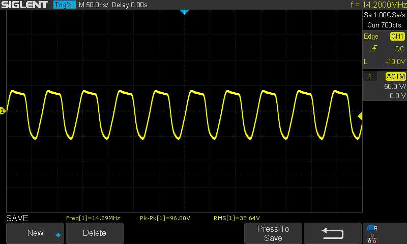
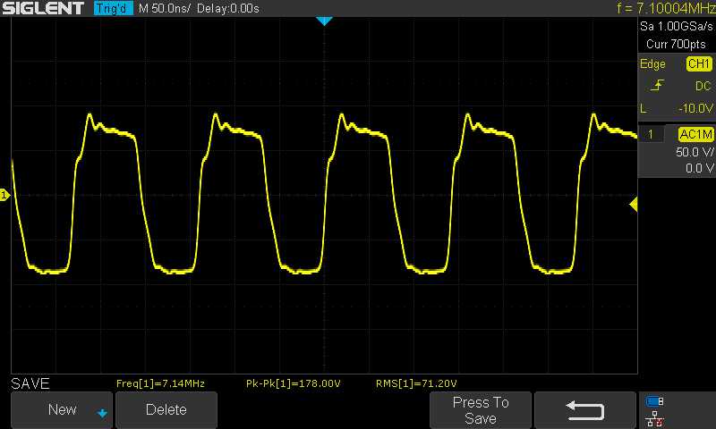
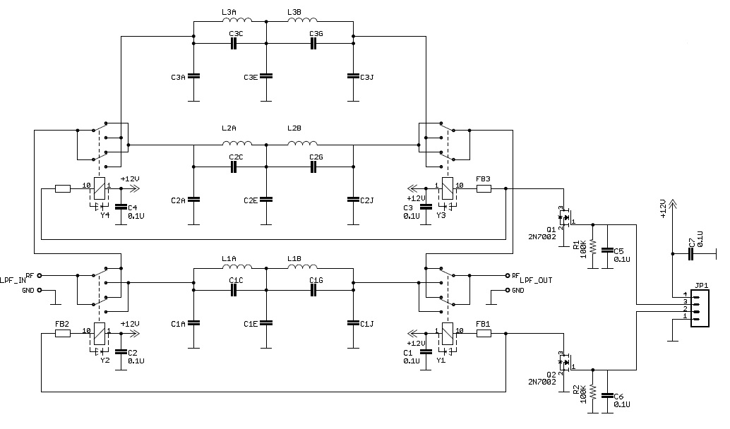
The author of the project Jim WA2EUJ suggested setting the quiescent current Iq to 100 mA. In my opinion, this value is too conservative, I checked that the effect on linearity is noticeable, so I increased the Iq to 200 mA. Below is the shape of the signal on a 50 ohm load connected to the output for 3650 kHz and a power of about 100 W. Current consumption from the 50 V power supply was 3.02 A, so the efficiency of the amplifier was 66.2%.

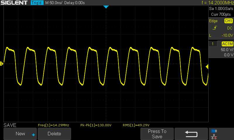
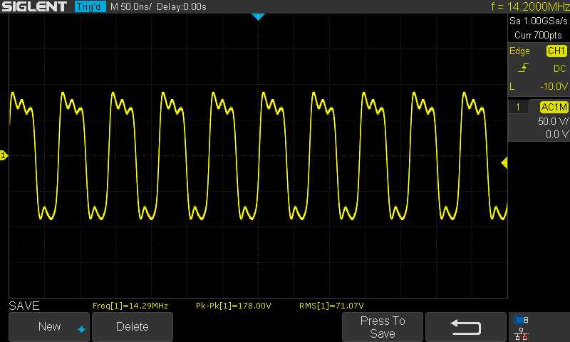
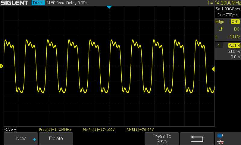
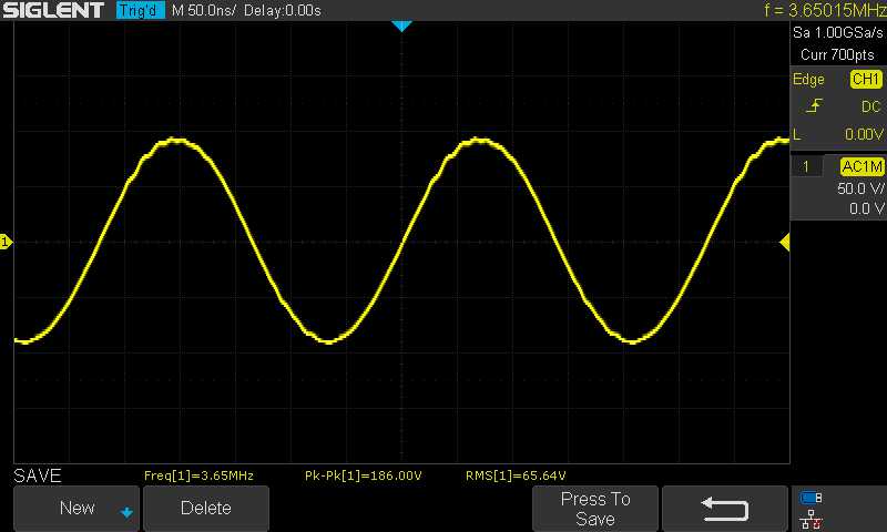
The following series of photos shows the effect of output power on the shape of the signal on a load of 50 ohms for 14200 kHz. It should be noted that the power value was calculated on the basis of the RMS voltage (visible under the oscillogram), so it is the total signal power with its harmonics. For estimation, I tried to use the function of determining the signal spectrum using the fast Fourier transform FFT, which is equipped with SDS 1202X-E. Unfortunately, the resolution of the reading of the peak values on the screen is poor. It can be estimated that for 100 W the first harmonic was about 13 dB lower than the basic one (i.e. at about 5 W), and the third about 23 dB lower than the basic one (i.e. at 0.5 W).

.
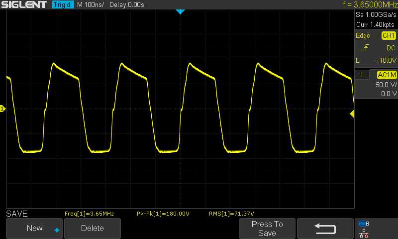
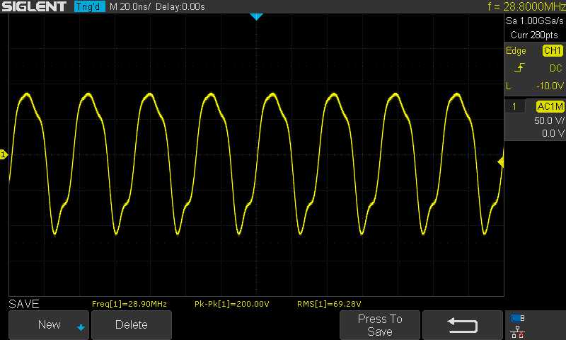
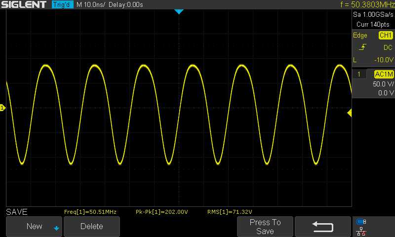
I checked the operation of the amplifier without bandpass filters on an artificial load in the range 1.8 – 52 MHz. I managed to get 100 W (according to the RMS voltage) in the full frequency range. The maximum control power did not exceed 1.2 W (based on SunSDR settings, not verified by the oscilloscope). This means a gain of about 20 dB – not bad! The following shows 100 W signals for various frequencies.

For further tests, I decided to make a bandpass filter for 80 m. Jim WA2EUJ developed the appropriate board in the same size 5×5 cm, the diagram of which is below. I installed the filter on the universal board only for the 80 m band, where the capacitances CA = CJ = 560 pF, CC = CG = 220 pF, CE = 1200 pF, LA = LB = 1.7 uH (17 turns on T68-2). The attenuation measurement on the second harmonic, i.e. 7.3 MHz with the help of a generator and oscilloscope, gave a result of 21 dB.
The signal for the 86 W output power is shown below. The current drawn from the power supply was 2.81 A, so the efficiency of the amplifier was 61.2%. Pretty decent! The maximum that I was able to “squeeze” was 93 W, but with very strong compression of the transient characteristics, which was noticeable above 80 W. I believe that 80W is a reasonable maximum useful output power value without falling into the range of large non-linearity of transistor operation. I was tempted to measure nonlinear distortions. The result was not super-accurate because the FFT function in the oscilloscope had low resolution, but it could be estimated that the second harmonic was more than 44 dB lower than the basic one – see below (the peak with a frequency 2.5 times higher is at a similar level – does can anyone explain it?). A test contact on the 80 m band was made (tnx SP5ELA), and no signal problems were found.
For further tests, I decided to make a bandpass filter for 80 m. Jim WA2EUJ developed the appropriate board in the same size 5×5 cm, the diagram of which is below. I installed the filter on the universal board only for the 80 m band, where the capacitances CA = CJ = 560 pF, CC = CG = 220 pF, CE = 1200 pF, LA = LB = 1.7 uH (17 turns on T68-2 ). The attenuation measurement on the second harmonic, i.e. 7.3 MHz with the help of a generator and oscilloscope, gave a result of 21 dB.
The project uses the MRF101AN transistor, there is its twin version MRF101BN in the mirror image package. This is a great idea that facilitates the construction of push-pull amplifiers. I think that such an amplifier with an output power of 200 W is relatively easy to do, I would like to check it. By the way, these transistors can also be used to make an 144 MHz band amplifier.
Jim WA2EUJ also developed the TX/RX switching system with SWR bridge. It is also made in a 5×5 cm module, which makes it possible to assemble a sandwich of all 3 tiles and keep the size of the whole small. There is also a 7-band version of the filters, but the board is 10×7.5 cm.
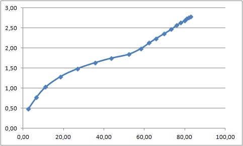
For supply Jim recommends easily available AC/DC 50V/200W switching power supply type EPP-200-48. You can also use two cheap 24V power supplies connected in series. If you are running on a 13.8 V car battery, a boost converter is required. You can easily find inexpensive DC/DC converters on auction websites. Good results with this amplifier can give a popular step-up converter module 1200 W with maximum input voltage ranges 10-60 V and output voltage 12-83 V. It may seem that 1200 W is overkill for a 100 W amplifier. But if the MRF101 amplifier at 50V power supply will require 4A in extreme cases (which is well below the inverter’s power and output current), then for 12 V at the input and assuming 90% DC/DC conversion efficiency, the inverter’s input current will be 18, 5 A. This value is close to 20 A, i.e. the maximum value of the input current of this step-up converter. For the model system powered by such a converter, I made a series of measurements for 3650 kHz:
![Pwy [W] vs. Pwe [W]](https://hf5l.pl/wp-content/uploads/2020/03/GNI-MRF-10.jpg)
![Wzmocnienie [dB] vs. Pwy [W]](https://hf5l.pl/wp-content/uploads/2020/03/GNI-MRF-12.jpg)

Razvan M0HZH solution – 600 W amplifier with MRF300 transistors won the second place in the “Homebrew RF Design Challenge”. This construction is definitely more technically interesting and more difficult to make. However, compared to known solutions, it is sensational simple and has excellent performance! Here also tempts me to make my version of such an amplifier.
If you need partially assembed PCB, please contact via qrz.com.
Miro SP5GNI
Number of Comments: 1
Thanks for the valuable information.
Hope we can make these amps And provide as kits .