
Personally, I think that a “real” SDR radio is one where the radio signal is received by the antenna and then (possibly after passing through passive filtering circuits) is sampled by an analog-to-digital converter. Further processing of the signal takes place in the digital domain. However, the SDR category also includes other devices which to a greater or lesser extent use digital signal processing. One of the uSDX transceiver variants described below is an example. It was created after reading an interesting article “QRP uSDX Transceivers”, which was published in Polish magazine “Świat Radio” No. 2/2021.
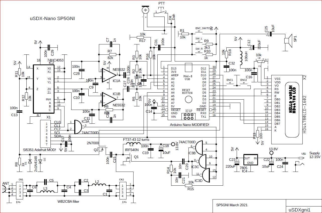
The uSDX project goes back to the products of the “QRP Labs” company. On the basis of the highly successful QCX mini-transceiver, Guido (PE1NNZ) came up with the uSDX design in order to try out what can be achieved with minimal system complexity by transferring it to implementation in the digital domain of the ATmega328P 8-bit microcontroller. The approach followed is to simplify the design where possible while keep a reasonable performance. The result is a cheap, easy to build, versatile QRP SSB/CW/digi transceiver that actually is quite suitable for making QSOs (even in contest situations), however due to the experimental nature some parts are still in progress and hence limited.
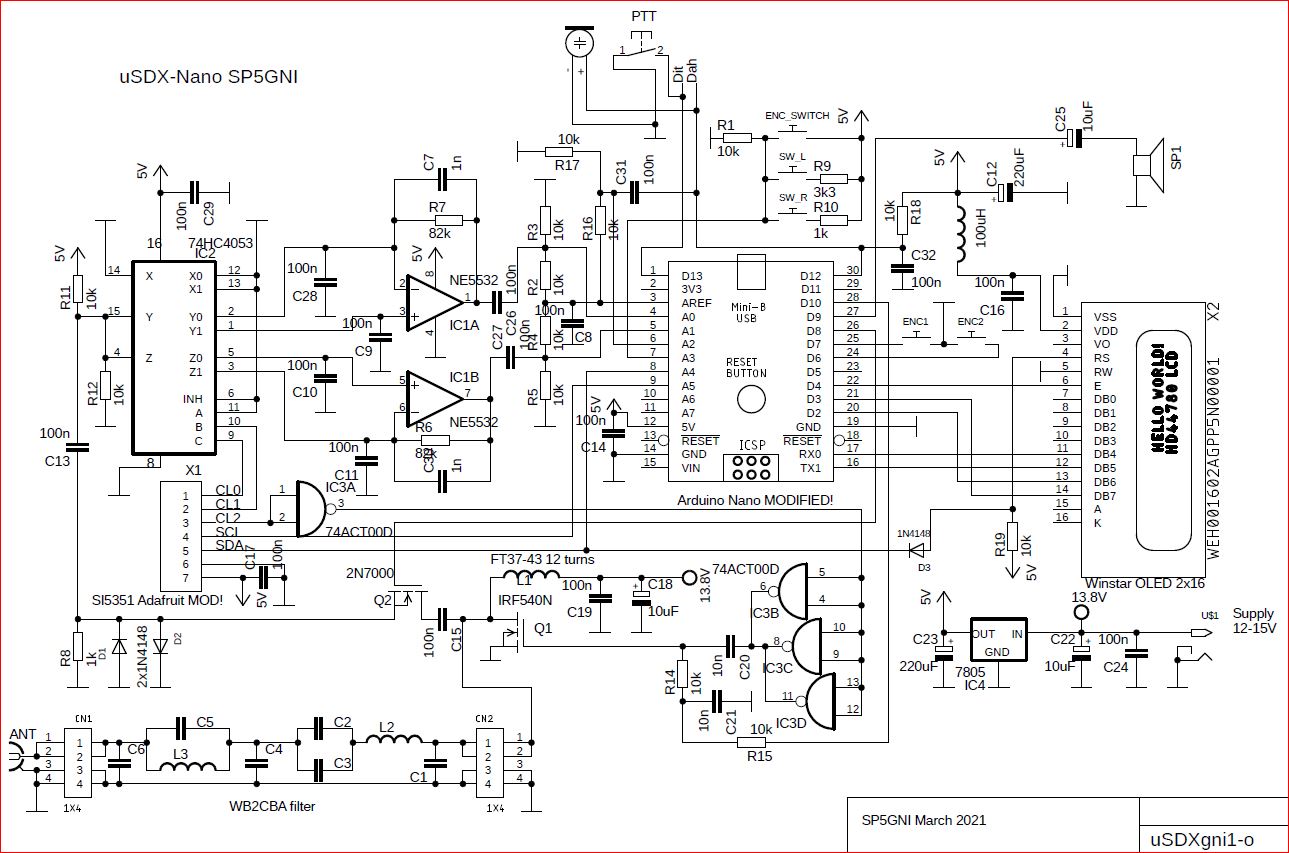
The receiver circuit is a direct conversion type. It uses the 74HC4053 IC as a high performance quadrature detector, also known as “Tayloe N7VE detector” or “I-Q mixer”. This detector is characterized by a very high value of the third order intercept point (IP3) and a large dynamic range, as well as low losses. In fact, we have 2 mixers here, which are keyed with signals with the operating frequency, but shifted between each other by 90 degrees. Clock signals CL0/CL1 for the detector are generated in the module containing the Si5351 type PLL frequency synthesizer circuit, which is controlled from the processor via the I2C bus.
There are several types of dual DIL-8 amplifiers on the market; the NE5532 shown in the schematic is readily available, but it works here in off-catalog conditions. Better to use an amplifier from the low-noise category LM4562, or even LT6231. Instead of the 74HC4053, the FST3253 is more often used as a quadrature detector. The resistance of the switch in it is much lower, so you need to limit the IC1A/B gain by adding 100 ohm resistors between C28 and pin 2 and between C11 and pin 6. The symmetry of both analog I and Q paths also affects the performance. It is good to match the components in such a way that their values in the groups are as close as possible to each other: C9/C10/C11 C28; R6/R7; C7/C30; C26 C27; R2/R3/R4/R5.
The output signals from the detector, after amplification and band-limiting by the IC1A/B dual operational amplifier, are fed directly to the inputs of the ATmega328P microcontroller analog-to-digital converter multiplexer, which is used in the Arduino Nano module here. Further processing of the signal takes place only in the digital domain, which is quite an achievement, considering the limited capabilities of the 8-bit microcontroller. The ATmega28P samples the ADC input at a 62kHz sample-rate, and decimates this high-samplerate to a lower samplerate, performs a phase-shift by means of a Hilbert-transform, summing the result to obtain side-band rejection; it subsequently applies a low-pass filtering, AGC and noise-reduction functions. With the 10-bit ADCs and a 4x over-sampling rate, a theoretical dynamic range of 72dB can be obtained in 2.4kHz SSB bandwidth. LSB/USB mode switching is done by changing the 90 degree phase shift on the CLK0/CLK1 signals of the SI5351 PLL. Three embedded attenuators are available for optimally using dynamic range; the first attenuator is the RX FET switch Q2 responsible for 20dB attenuation, the second attenuator is ADC range (1.1V or 5V) selected by the ATMEGA ADC analog reference (AREF) logic and is responsible for 13dB attenation, the third attenuator is a pull-down of an analog input on the ATMEGA with a GPIO port responsible for 53dB attenation. Combining the three attenuators provides the attenation steps 0dB, -13dB, -20dB, -33dB, -53dB, -60dB, -73dB. The receiver circuit does not have an analog headphone amplifier – a digital output with PWM pulse width modulation is used. The audio signal is strong enough, even a small speaker with an impedance of 8 ohms can be used.
The SSB transmit-stage is implemented entirely in digital and software-based manner: at the heart the ATmega328P is sampling the input-audio from the electret microphone and reconstructing a SSB-signal by controlling the SI5351 PLL phase (through tiny frequency changes over 800kbit/s I2C) and controlling the PA Power (through PWM on the key-shaping circuit). In this way a highly power-efficient class-E driven SSB-signal can be realized; a PWM driven class-E design keeps the SSB transceiver simple, tiny, cool, power-efficient and low-cost.
The Arduino module additionally supports a 2×16 character LCD display, buttons and a rotary encoder (pulser with a switch). The entire transceiver is powered by 5V through the 7805 stabilizer, except for the E-class power amplifier, powered directly by the input voltage – typically 13.8V.
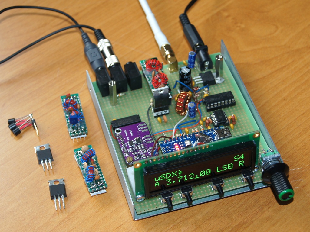
The layout is so simple that I decided to assemble it on a universal printed circuit board. I used the mechanical concept of my GNI-r8 rotor controller with a 2×16 OLED display.
Source codes (open source), detailed principles of operation and documentation of the originator of the project, Guido PE1NZZ, are available on GitHub https://github.com/threeme3/QCX-SSB and https://github.com/threeme3/QCX-SSB/tree/feature-rx-improved . In addition to the theory and diagram, there is also a description of the software command menu. In a short time, the project found many enthusiasts gathered in the group on the forum https://groups.io/g/ucx . The project is under constant development, in various variations and versions. My scheme is mainly based on solutions of: Barb WB2CBA https://antrak.org.tr/blog/projeler/usdx-an-arduino-based-sdr-all-mode-hf-transceiver-pcb-iteration-v1-02/ , Manuel DL2MAN https://dl2man.de/ and Miguel PY2OHH https://www.qsl.net/py2ohh/trx/usdxnano/usdxnano.html . It’s also worth taking a look at Bob’s KD8CGH website https://sites.google.com/view/kd8cgh/Home/introduction-to-the-usdx .
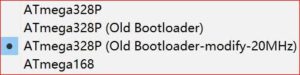
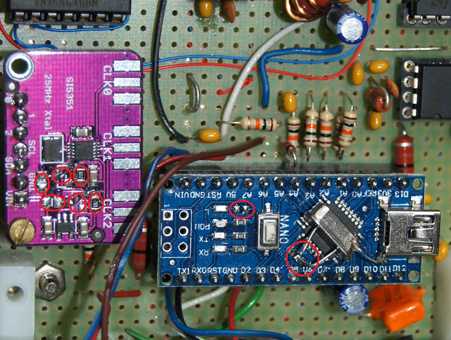
Instead of the Arduino Nano module in other uSDX variants, the ATmega328P processor in the DIL package is most often used. In this case, a 20MHz crystal is connected to it, and an additional programming interface must be provided (or the microcontroller must be programmed after removing it from the socket). In my case, the Arduino module can be programmed directly via a USB cable. The module, however, requires a modification. The original 16 MHz quartz must be exchanged for 20 MHz and the SMD resistor attached to the LED (marked L) must be removed. After such conversion, it is no longer possible to program from a computer from the Arduino IDE environment, unless the method of direct programming the Arduino Nano 20MHz via the Arduino IDE proposed by PE1DDA is followed:
1.Find the file named boards.txt from arduino IDE, it is located in the fold like “home of arduino\hardware\arduino\avr”.
2.Edit boards.txt.
2.1 Find the line: nano.name = Arduino Nano
2.2 Copy the lines from “## Arduino Nano w/ ATmega328P (old bootloader)” down to “nano.menu.cpu.atmega328old.build.mcu=atmega328p”
2.3 Paste these lines below “nano.menu.cpu.atmega328old.build.mcu=atmega328p”
2.4 In each line, replace atmega328old with “atmega328old20MHz”
2.5 Replace this line “nano.menu.cpu.atmega328old20MHz=ATmega328P (Old Bootloader)” with “nano.menu.cpu.atmega328old20MHz=ATmega328P (Old Bootloader-modify-20MHz)”
2.6 Edit this line “nano.menu.cpu.atmega328old20MHz.upload.speed=57600”, replace with “57600” with “72000”
2.7 Save and close the boards.txt file
3.Run the Arduino IDE: Tools, Arduino Nano Board, Board Manager …, click Update,
4.Restart Arduino IDE, you can find a new board as shown below
Now you can upload programs to Arduino Nano with 20MHz from IDE via USB directly.
The Si5351 frequency synthesizer module also requires some rework. It is controlled from the microcontroller via the I2C bus with an above-standard speed of 800 kbit/s, and the voltage translator circuits used there are too slow. You need to remove 2 FET SMD transistors and 4 10k SMD resistors. Then install two 1k SMD resistors and two jumpers between the drain and the source instead of FET transistors. The appearance of both modules after the modifications is shown below.
Three 74ACT00 gates in parallel were used to drive the Q1 power transistor. These may be other gates, but necessarily from the ACT – HC or HCT series do not have enough current capacity to drive the PA amplifier transistor well. On the forum https://groups.io/g/ucx you can find a number of other proposals for controlling the output transistor, but my experience confirms that 3 parallel 74ACT00 gates seem to be the optimal solution, also due to the relatively good availability of these ICs.
The situation is similar with the Q1 transistor – you can follow various options on the forum mentioned above. I had BS170, 2N7000, IRF510, IRF540N and IRF610 at my disposal. The IRF540N worked best for me on the 80m and 40m bands, and 3 2N7000 connected in parallel on the 20m band. It’s worth checking out other options.
In order to obtain the appropriate output power, the output circuit is very important for a class E amplifier. By design, it is a resonant amplifier. I chose to use one of the WB2CBA solutions, which seems to be a good compromise between quality and simplicity. In order to obtain satisfactory results, I had to adjust the values of the circuit parameters. I must make it clear that the values given below are not necessarily optimal values. First of all – their values strongly depend on the type and even the unit of the transistor, construction and load. I made tests with a 13.8V power supply with an artificial load of 50 ohms until I was satisfied with the results I considered:
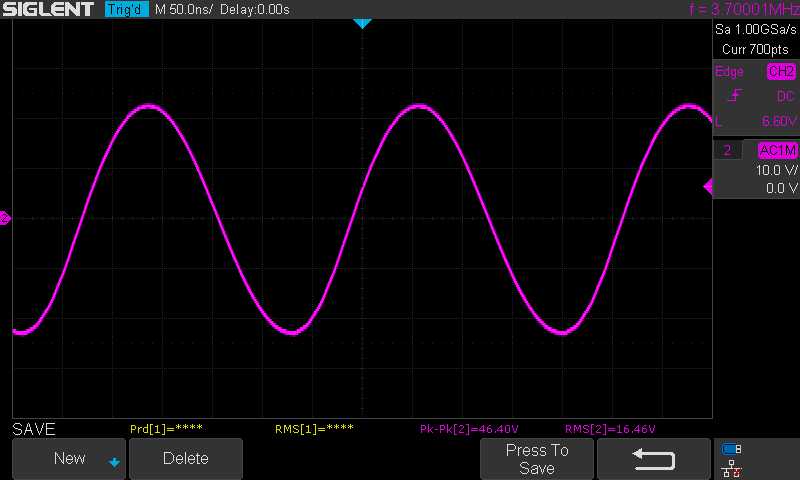
3.700 MHz power 5.8 W, efficiency 76% (IRF540N)
3,500 MHz, power 9.4 W, efficiency 78% (IRF540N)
7.100 MHz, power 8.8 W, efficiency 93% (that’s how I came out of the calculations!) (IRF540N)
14.200 MHz, power 2.7 W, efficiency 56% (3x 2N7000)
Below is a screenshot of the output oscilloscope on an artificial load for the 80m band. I have not measured the harmonic content, but the signal looks quite “clean”. Next to it is the RF signal on the Q1 drain. As you can see, the Q1 transistor works in the keying mode. The drain current flows when the voltage across it is close to zero, which ensures high gain efficiency. This is shown very nicely in the article https://people.physics.anu.edu.au/~dxt103/160m/class_E_amplifier_design.pdf . As you can see, the voltage value reaches 81.6V. Miguel PY2OHH made tested with a supply voltage of up to 32.5V. For the 80m band it gave 20W output power with 75% efficiency. The drain voltages are therefore much higher, hence the Q2 2N7000 transistor must be replaced with a more resistant one, eg IRF510. You cannot forget about the D1 and D2 protective diodes!

The original WB2CBA series resonant filter solution is available at https://antrak.org.tr/blog/usdx-multiband-low-pass-filter/ . The component values for the three most popular bands are given below. The values that I have changed from the original are in bold. The L1 choke is 12 turns on the T50-2 ring core (not FT37-43 as shown on the schematics!). The L2 and L3 inductances can be wound with a winding wire 0.2-0.4mm or a wire with insulation (e.g. kynar as in the photo above) on T37-2 cores.
| Band | C1 | C2 | C3 | C4 | C5 | C6 | L2 | L3 |
| 80 m | 680pF | 360pF | 1,5nF | 1,8nF | 620pF | 1,8nF | 15 t. | 15 t. |
| 40 m | 360pf | 180pF | 470pf | 1nF | 180pF | 1nF | 12 t. | 10t. |
| 20 m | 100pF | 470pF | x | 470pF | 150pF | 470pF | 8 t. | 7 t. |
I made filters in the form of plug-in modules. There are a number of examples and ready-made solutions of multi-band output circuits with switches or relays in the network, e.g.: https://dl2man.de/bottom-layer-rf-board/ .
The original source code for ATmega328P is available for download on GitHub https://dl2man.de/bottom-layer-rf-board/ . I checked several versions of the program in my uSDX system, it is worth looking for the latest one, e.g. HERE. In order for the program to work on Arduino Nano, it was slightly reworked. In version v.1.02p I changed only 2 lines:
line 12: //#define CAT 1 // GNI blocked, CAT-interface (CAT takes a lot of memory space)
(CAT function disabled to free memory resources of the microcontroller)
line 15: #define F_XTAL 25000373 // GNI changed, 25MHz SI5351 crystal (enable for 25MHz TCXO)
(the value was adjusted experimentally for my Si5351 module)
In my uSDX prototype, I used a more modern 2×16 OLED display. It worked in my rotor controller https://hf5l.pl/wp-content/uploads/2020/11/User-manual-EN_r8_v03.pdf . For it to work properly, I had to add D3/R19 parts. In the case of a standard LCD with backlight, they are not needed, but you need to add a potentiometer to adjust the contrast and a resistor for the backlight as shown in the diagram below.
After programming the module in the Arduino IDE (Nano – Atmega328P – Old Bootloader-modify-20MHz)) and placing it in the socket of the assembled transceiver, first set the display contrast using the 10k potentiometer. There are 3 buttons to operate the radio: left L, right R, ENC encoder button and a mechanical rotary encoder (the encoder button can be doubled with a micro-switch, which requires much less pressure and is more convenient to use). The buttons have the following functions (x means press, 2x double press, d long press):
L x – entering the menu and sub-menu
R x – mode change: LSB (lower band), USB (upper band), CW and exit from the Menu
R 2x – change of reception bandwidth: Filter Full, 3000 Hz, 2400 Hz, 1800 Hz (different for CW)
R d – change of VFO A, RIT, VFO B, RIT
ENC x – tuning step: 1M, 100k, 10k, 1k, 500, 100, 10 Hz
ENC d – tuning step: 10 Hz 100, 500, 1k, 10k, 100k, 1M,
ENC 2x – band-switch to pre-defined CW/FT8 frequencies on successive amateur bands
ENC + turn – changes the volume.
So in short – tuning can be done by turning the rotary encoder. Its step size can be decreased or increased by a short or long ENC press. A change of band can be done with a double ENC press. The mode of operation is altered with a short press on the right button; a double press on right button narrows the receiver filter bandwidth, the bandwidth is reset every time mode is changed. The volume is changed by turning the rotary encoder while pressed. The content of the menu slightly depends on the version of the program, descriptions of its functions can be found in the documentation, e.g. : https://github.com/threeme3/QCX-SSB/tree/feature-rx-improved .
For receive, by default an AGC is enabled (item 1.8 in menu). This increases the volume when there are weak signals and decreases for strong signals. This is good for SSB signals but can be annoying for CW operation. The AGC can be turned off in the menu, this makes the receiver less noisy but require more manual volume change. To further reduce the noise, a noise-reduction function can be enabled in the menu with the NR parameter (1.9 in menu). To use the available dynamic range optimally, you can attenuate incoming signal by enabling a front-end attenuator with “ATT” parameter (1.10 in menu). Especially for frequencies 3.5-7 MHz the atmospheric noise levels are much higher, so you can increase the receiver performance by adding attenuation (e.g -13dB) such that the noise-floor is still audible.
A S-meter of choice (dBm, S, S-bar) can be selected with the S-meter parameter. Selecting an S-bar, shows a signal-strength bar where each tick represents a S-point (6dB).
To calibrate the transceiver frequency, you can tune to a calibrated signal source (e.g. WWV on 10 MHz) and zero-beat the signal by changing “Ref freq” parameter (8.1 in menu).
For FT8 (and any other digital) operation, select one of the pre-programmed FT8 bands by double press the rotary encoder, connect the headphone jack to sound card microphone jack, sound card speaker jack to microphone jack, and give a long press on right button to enter VOX mode. Adjust the volume to a minimum and start your favorite FT8 application (WSJT-X for instance). The sensitivity of the VOX can be set in the “VOX threshold” parameter.
The values of the transmitter parameters are best chosen experimentally. The TX Drive value (pos. menu 3.3) is normally used in the range 4-6 (my 6). Having an oscilloscope is helpful to observe the modulation envelope of the signal at the output. Eavesdropping on another receiver does not work. The signals generated by the digital circuits on the uSDX board overlap the useful signal, which makes it seem very distorted and it is impossible to assess the real quality of the SSB signal at the antenna output. PA Bias min (item 8.1) in my opinion does not matter much (I have 10). PA Bias max (item 8.2) can be selected in the following way: in CW mode, we simultaneously observe the signal on the artificial load and the current drawn from the power supply; using the encoder, we increase the value of the PA Bias max parameter until a further increase in current does not result in an increase in output power. For me the value of PA Bias max = 105 came out.
I checked the operation of my transceiver on the air. The farthest connections on the SSB were IZ2LSR at 80m (1,130km), YU1XA at 40m (950km), EC5K at 20m (2,200km).
Have fun installing and using the uSDX transceiver. However, it should be remembered that this is an experimental solution and has a number of limitations resulting not only from the simplicity of construction. It is worth checking new ideas and solutions on the web, e.g. here: https://github.com/KD9PDP/uSDX-x . The finished boards have already been developed by several colleagues and should be available, e.g. here: https://www.hamshop.cz/usdx-c57/dl2man-sandwich-oled-partially-assembled-i403/ .
Mirek SP5GNI
Number of Comments: 47
Thank you for sharing, I have posted the link in my FB wall.
https://www.facebook.com/groups/uSDXQrp
WJ6C/exCO6BG
Hello. I set up the circuit but compared to TS2000 and FT950 commercial radio, the reception level is quite low, I don’t know if you even compared it to commercial radio. Some colleagues said that they also noticed this deficiency in reception.
73 // Francisco- PY2OV
py2ov@yahoo.com.br
Taking into account the simplicity of the uSDX design, it is difficult to expect results fully comparable with the factory equipment.
Miro SP5GNI
Hi dear Miro
Is it possible to send me the code as you made it?
In order to use a standard 2×16 lcd display is there a need to change something in the code ?
Thanks
George sv1elf
Hi! The inductor showed in your photo of the mainboard does not have a T37-43 core… I’m sticking with the T37-43 12 turns to begin with…. What core and how many turns are you using actually and why? Thanks! LU1AAX Mauricio
Yes, you are right. I used T50-2 instead of T37-43.
For filters I was using T37-2.
Miro SP5GNI
So the inductor should be 12 turns on T50-2 core?
Yes, it worked for me.
Miro SP5GNI
Hi Miro, I have ended mounting the mainboard circuit. I will prepare a 40 m band filter. I can check the transmitter is working OK getting a signal (of course weak) at Q1 gate. I put an IRF540 and a dummy load at the output and I am getting a few milliwatts of output (less than 500)… I am rereading your article and you say that the ouput is important to this resonant amplifier design so the question is how could I test this before ending the LPF filter for the intended working band?
Hello
Class E amplifier needs resonat load. Transistor is switched on only during a short part of period and you need resonant circuit to seperate out the first harmonic.
If you have an osciloscope you can observe the output and find optimum LC values. It depnds also on transistor type. IRF540 is produced in many places and in many series. I found that IRF540N was the best.
Miro
Hi Miro, in your IRF540N you are reaching voltage values that rule out using common 50V capacitors… I think a mention about this is worth in the main article… Greetings from Mauricio LU1AAX
Hi Miro, I’m in the final stages of builing this nice project… I replicated your filter values with my IRF540N and it works awful. I think those values are tied to your particular transistor unit. So I used this spreadsheet to build a filter for an IRF510 http://www.wa0itp.com/class%20e%20design.html, where “out of the box” I could get 3W output in CW but when I switch to SSB I cannot put an intelligible signal unless I use a PA bias value of around 15 (and then the audio is quite noisy which makes me suspect of the quality I am getting from the mic audio feed)… a higher value increases power output but at the expense of great distortion to the point of the signal not being detected by a nearby receiver.
I have some doubts about how is audio from the mic acquired, and I’d like to check with you that I am getting it right. +5V to the mic are provided by circuit line tied to +5V through pullup R18… D12 (pin 30) seems to sense DAH while audio from the mic makes its way through C31 to A2 (pin 16) where analog audio is sampled by the microcontroller. So if I want to check what audio I am feeding I better put my oscilloscope probe at A2 and see what’s going on there, right?
Yes, A2 is good for checking audio. For SSB R18 is used for electret microphone bias.
What I don’t understand is why AREF is also tied to the mic audio trough R13… I’m completely lost here… looks like you sample mic audio at A2 while simultaneously varying AREF voltage (?)
Do you mean R16?
All ADC inputs are biased with half of the ADC reference voltage. It is needed for AC signals conversion.
I had a similar feeling when I listened the signal on my receiver nearby. But you have to remember that such a receiver also catches signals generated directly from the Adruino PCB. To assess the quality of the SSB signal, it is best to use a web SDR receiver, or ask a colleague at least a few kilometers away.
In my device I use PA bias min 10, PA Bias max 150, TX Drive 4.
Miro SP5GNI
Hi Miro, I’m experimenting this problem: CW is ok, but in SSB when I PTT the Tx goes almost full power with noise… I’m tracking the issue down to finding a carrier at SIS5351 CLK2 when no signal even though the audio signal from the mic is not noisy. Do you experience none or little power when you PTT your rig? I’ve checked out the circuit looking for some assembling error but found none. There was a similar problem in the past that PY2OHH solved placing a MOSFET between the ACT00 and the main MOSFET but it says the issue was solved in software version M. There was Tx activation but I understand it was not at almost full power like happens in my case.
10nF from A2 to GND seems to fix the RF flooding but the mic input is still noisy.
Hi
Try to experimet with settings: TX Drive, PA bias…
Miro SP5GNI
Achei interessante, no entanto desatualizado tecnologicamente. Já existe Arduino bem mais rápido e CIs mais modernos e mais eficientes.
Poderia fazer um retrofit nesse projeto para ficar supimpa.
You are not getting the point of this project. It is about building a usable transceiver with minimum hardware and relying mostly in software processing. You cannot call “desatualizado” a project that’s a leading edge on producing a SSB signal just in software with just a small microcontroller like the atmega328p and a few more ICs pushed to the limit of their specs.
DL2MAN and PE1NZZ have a talk on 14th Nov 2021 on Hamfest India 2021
We got to see a prototype of the uSDX Final Version!
It was a 90 Minute presentation explaining the history, schematics & discussion the future roadmap of uSDX
https://itshamradio.com/sneak-peek-of-usd-final-version-by-dl2man
Thank You Saquib for providing the info!
It was very interesting to see and listem to Manuel and Guido.
Miro SP5GNI
Hi Miro,
First of all, thanks for this project!
I have modified the Arduino Nano with a 20 MHz xtal. It runs the previously uploaded code (1.02j). However when I made the required modifications to boards.txt and tried to upload new code I got an out of sync error. The oscillating frequency actually is 20060 MHz, so I tried as well 72216 instead of 72000. Then I tried other values around, 72100, 72150, 72200, 72250, 72300, but no joy.
Any hints?
Thanks in advance.
73
António CT1CXP
Hi Antonio
check again your boards.txt file and look for errors, like typo.
I can send you my file for trying, if you want.
Miro SP5GNI
Hi Miro,
Thanks! I double checked, but I don’t find any problem in the file. But I would appreciate to test yours, so please send it to me.
I am suspecting that the XTAL might not be oscillating at the right frequency, although I get a spectrum spike at 20.060 MHz with Arduino on.
Best 73
António
CT1CXP
Ho un uSDX+ hf .ho un problema per il microfono .quando trasmetto in lsb o in usb la modulazione non e’ buona .penso che dipenda dal mdulatore dl TX .Se qualcuno sa dirmi qualche cosa in merio al difetto. Grazie
Hi Maurizio
I have answered already before for similar post:
I had a similar feeling when I listened the signal on my receiver nearby. But you have to remember that such a receiver also catches signals generated directly from the Adruino PCB. To assess the quality of the SSB signal, it is best to use a web SDR receiver, or ask a colleague at least a few kilometers away.
In my device I use PA bias min 10, PA Bias max 150, TX Drive 4.
Google traslator:
Ciao Maurizio
Ho già risposto prima per un post simile:
Ho avuto una sensazione simile quando ho ascoltato il segnale sul mio ricevitore nelle vicinanze. Ma devi ricordare che un tale ricevitore cattura anche i segnali generati direttamente dal PCB Adruino. Per valutare la qualità del segnale SSB è meglio utilizzare un ricevitore web SDR, oppure chiedere a un collega distante almeno qualche chilometro.
Nel mio dispositivo utilizzo PA bias min 10, PA Bias max 150, TX Drive 4.
Miro SP5GNI
Hi Miro,
Do you think a unmoded Si535351 Adafruit board could handle FT8 mode? I don’t plan on using SSB, voice, and hoping that the FT8 frequency changes would be slow enough to work.
Just planning on CW and Digital.
73s Jack
W6VMJ
Hi
FT8 is much simpler than SSB! I found quite a lot of examples:
https://forums.adafruit.com/viewtopic.php?f=19&t=157153
https://www.reddit.com/r/amateurradio/comments/l9m25l/homebrew_ft8_transceiver/
https://hackaday.com/2021/09/25/the-simplest-ft8-transceiver-youll-ever-build/
https://twitter.com/lu2hes/status/1211797537641967616
…
Miro SP5GNI
I used my ft857D to observe the (absence of) quality of the ssb signal coming out of these radios (I have the uSDR and the uSDX+). usdx connected to dummy load, yaesu with just a wire close by, The audio received was just terrible. impossible to understand what was modulated. But I heard people making contacts with these. Reports were ok. Not super audio but intelligible. After trying with 2 other receivers, I tried to lower the rf gain on the yaesu…to the minimum and cranked it up slowly…That was the problem all along. I can hear proper ssb speech coming out of the little radios now! Try it! you will be surprised at how (not bad at all) they sound!
uSDR: Noise Gate=3 TX Drive=4 PA bias min=10 PA bias max=130 IQ phase=93
To adjust the IQ phase, I transmitted in a dummy load @ 5 watts in a dummy load @ 3500khz cw USB with the yaesu. Just holding the radio in my hand(not connected to the yaesu) with a dangling piece of wire in the BNC, Tuned the uSDR in LSB @3500khz and adjusted the IQ phase for minimum signal(completely disappeared actually). In a direct conversion SDR receiver, Balancing the I & Q signals serves to eliminate the opposing sideband.(sideband rejection)
Have fun with these little radios !
No need to carry big batteries
Yaesu FT857D…RX=780 miliamps
uSDR…RX=94 miliamps
uSDX+…RX=81 miliamps with the lamp off…86 miliamps with it!
Hi.
Collected according to this scheme. But I did not change the quartz in the arduino nano, and did not modify the si5351. Installed an OLED display. When turned on, the diagnostics pass, !!V3.3=4v, !!Vavcc=5v. Shows the frequency and only a squeak sounds from the speaker. What to do?
Thanks.
The original code was written for the Atmega328 processor with a 20MHz clock, I’m afraid that 16MHz is not enough to properly form the SSB signal.
The Si5351 synthesizer module is controlled from the microcontroller via the I2C bus much faster than I2C standard speed, and the voltage translator circuits used there would not work at all. You need also remember about the difference in logic levels. The proposed change is in my opinion the simplest, but you can find also other solutions of the problem.
Miro SP5GNI
Hi Miro,can you sendme your boards.txt with 20MHz mod?
yo2lqa@gmail.com
Thank you.
73 Op.Zoli
Good morning.
Can I use 50v capacitors in the LPF filter, considering the use of bs170 transistors in the RF amplifier?
If so, what is the maximum power that I can apply?
Which bias parameters to use?
Grateful
Daniel PX2r7379
Hi Daniel
The peak voltage at the drain of a power transistor can be quite high. I would recommend that at least C1 be for 100V.
Output power can’t be predicted, try to optimize the circuit and parameters. According bias I use 10, you can experiment with it as well.
Miro SP5GNI
Hi Miro SP5GNI.
Thanks for answering. I really hadn’t paid attention to the peak voltages of the uSDX’s PA stage, reading a little more about it I could see that 50V capacitors are somewhat inadequate. I’m in Brazil and I’m having trouble finding capacitors with a higher voltage, at least 500v. I’m going to try the 100v ones and leave everything at minimum to have a satisfactory output power.
Thanks again for answering me.
73 Daniel px2r7379
You can use simple trick and connect two 50V-capacitors in series (for example 2x200pF instead of 100pF)
Miro
Hi Miro.
I know the association of capacitors to form an equivalent and I will use this trick without a doubt. I just think that this arrangement is a little bulky on the pcb, but that’s ok, if there’s no other way I’ll do it.
Once again thanks for the help
73 Daniel Px2r7379
Hello Miro, I’m looking at the circuit and I see the use of the 74act00, according to the logic if the state is low its output is high and if its state is high it is also high, but since its inputs are linked, whatever its input, it always Its output will be high, so I do not understand when its action is in the diagram, I can replace this IC with a SNCTLV1G125, it is a simple mosfet key and much faster, if necessary I could use 2 of these and put a 74act04 in front of one of them to invert the signal, that way it would work the same as a 74act00.
For the 74hc4053 I will use a much faster SN74LVC1G3157.
Thank you in advance Mario LU1TAL, Jujuy, Arg.
Hi Mario
Logic functionality of the gates is not important at all. The gates are used as drivers for MOS power transistor. The driver must be as fast as possible, and should have enough output power to drive the MOS (in practice to reload MOS input capacitace, which is pretty high). 3 gates in parallel are also important for better driving.
ACT series was chosen for the best results. If you want – place the socket and try different series – let me know about results.
Miro SP5GNI
Ok Look, now I understand the function of the 74AC00 key, I think my 74lvc1g125 switches will work perfectly,
I will finish my QRP soon and I will tell you about my experiences, thank you very much, 73
Hi Miro,
Thank you for putting up your very clear explanation of the usdx. I am starting to put together mine but, after programming, on my 2×16 LCD screen I am only getting a cursor on the bottom line (which I can move around with the rotary encoder push button switch) and black boxes on the top line. The problem may be with my Si5351 board modifications and not the display. My question for you is does the Si5351 board have to be functional in order to get the rest of the code to work? By that I mean does the program hang (hence my strange display results) if it sees an issue on the 12c?
Thank you for your help, George WA1PDY
Hi George
what kind of LCD do you use? If standard – then use uSDXgni1 schematic without D3/R19. If OLED – use uSDXgni1-o schematic.
Are you sure about the load coil “L1 choke is 12 turns on the T50-2 ring core (not FT37-43 as shown on the schematics!)”, that would be just 0.71 uH, did you mean T50-61, 12T = 9.9uH
Rob, yes, I used T50-2 instead of T37-43.
Miro